2. CREATING THE HARDWARE PLATFORM
In the previous chapter, we have defined the structure of the microprocessor based system that will be used as a part of the solution of PWM signal generation. In this chapter, we will explain how to generate this system using Vivado IP Integrator tool. While entire designs can be created using the IP Integrator, the typical design will consist of HDL, IP and IP integrator block designs.
2.1 Create a New Project
The first step in creating a new design will be to create a new project. We will crate a new project using the Vivado IDE New Project wizard. The New Project wizard will create an XPR project file for us. It will be place where Vivado IDE will organize our design files and save the design status whenever the processes are run.
To create a new project, follow these steps:
-
Launch the Vivado software:
Select Start → All Programs → Xilinx Design Tools → Vivado 2014.2 → Vivado 2014.2 and the Vivado Getting Started page will appear, see Illustration 2.1
As you can see from the illustration below, the Getting Started page contains
a lot of usable links (shortcuts) like Create New Project, Open an existing Projects, Open Example Project, Open Hardware Manager, Documentation and Tutorial and so on, see Illustration 2.1
- On the Getting Started page, choose Create New Project option
- In the Create a New Vivado Project dialog box, click Next and the wizard will guide you through the process of a new project creation, see Illustration 2.2
-
In the Project Name dialog box specify the name and the location of the new project:
- In the Project name field type modulator as the name of the project
- In the Project location field specify the location where project data will be stored
- Leave Create project subdirectory option enabled, see Illustration 2.3
- Click Next
- In the Project Type dialog box specify the type of project you want to create. In our case we will choose RTL Project option. Select Do not specify sources at this time also, see Illustration 2.4
- As you can see from the Illustration above, four different types of the project can be created:
- RTL Project – The RTL Project environment enables analysis of the compiled RTL design including logic exploration, resource and power estimation, DRCs, and I/O pin planning.
- Post-synthesis Project – This is where pre-implementation design analysis, debug core insertion, and constraint definition is performed. You can explore various constraints sets, devices, and implementation options.
- I/O Planning Project – This type of project do not specify design sources. It is intended for early pin testing.
- Imported Project – The Implemented Design environment loads the netlist and implementation results directly from the run directory to ensure that the viewed data represents the launched run.
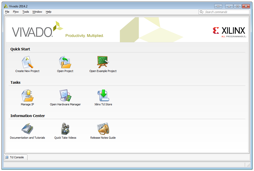
Illustration 2.1: The Vivado Getting Started page
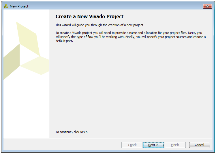
Illustration 2.2: Create a New Vivado Project dialog box
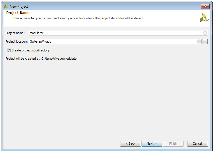
Illustration 2.3: Project Name dialog box
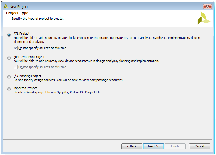
Illustration 2.4: Project Type dialog box
- Click Next
- In the Default Part dialog box choose a default Xilinx part or board for your project. Select Boards to choose the default board for the project and a list of evaluation boards will be displayed, see Illustration 2.5
- Select Kintex-7 KC705 Evaluation Platform as it is shown on the illustration above
- Click Next
- In the New Project Summary dialog box click Finish if you are satisfied with the summary of your project. If you are not satisfied, you can go back as much as necessary to correct all the questionable issues, see Illustration 2.6
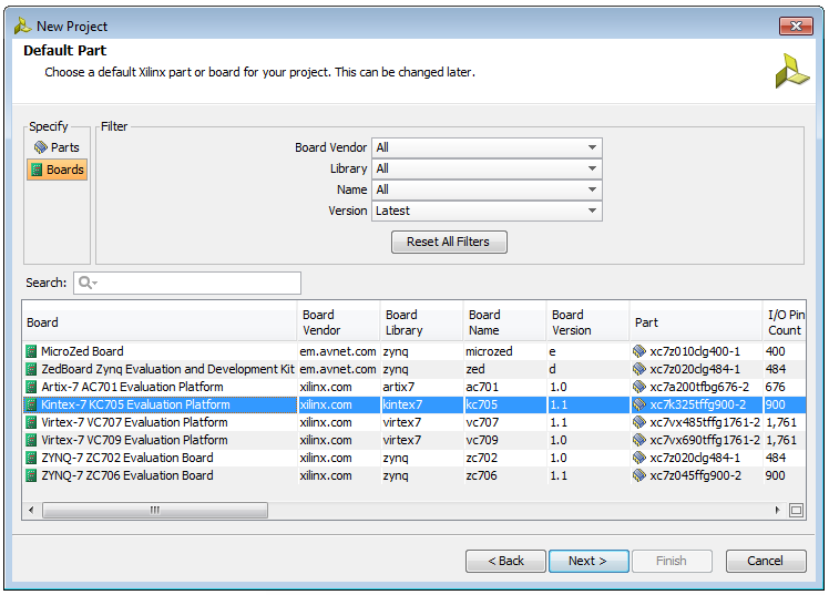
Illustration 2.5: Default Part dialog box
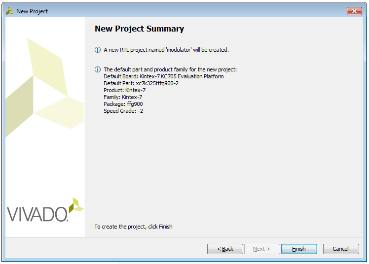
Illustration 2.6: New Project Summary dialog box
After we finished with the new project creation, in a few seconds Vivado IDE Viewing Environment will appear, see Illustration 2.7.
When Vivado creates new project, it also creates a directory with the name and at the location that we specified in the GUI (see Illustration 2.2). That means that the all project data will be stored in the project_name (modulator) directory containing the following:
-
project_name.xpr file – object that is selected to open a project (Vivado IDE
project file)
- project_name.runs directory – contains all run data
-
project_name.srcs directory – contains all imported local HDL source files,
netlists, and XDC files
- project_name.data directory – stores floorplan and netlist data
- project_name.sim directory – contains all simulation data
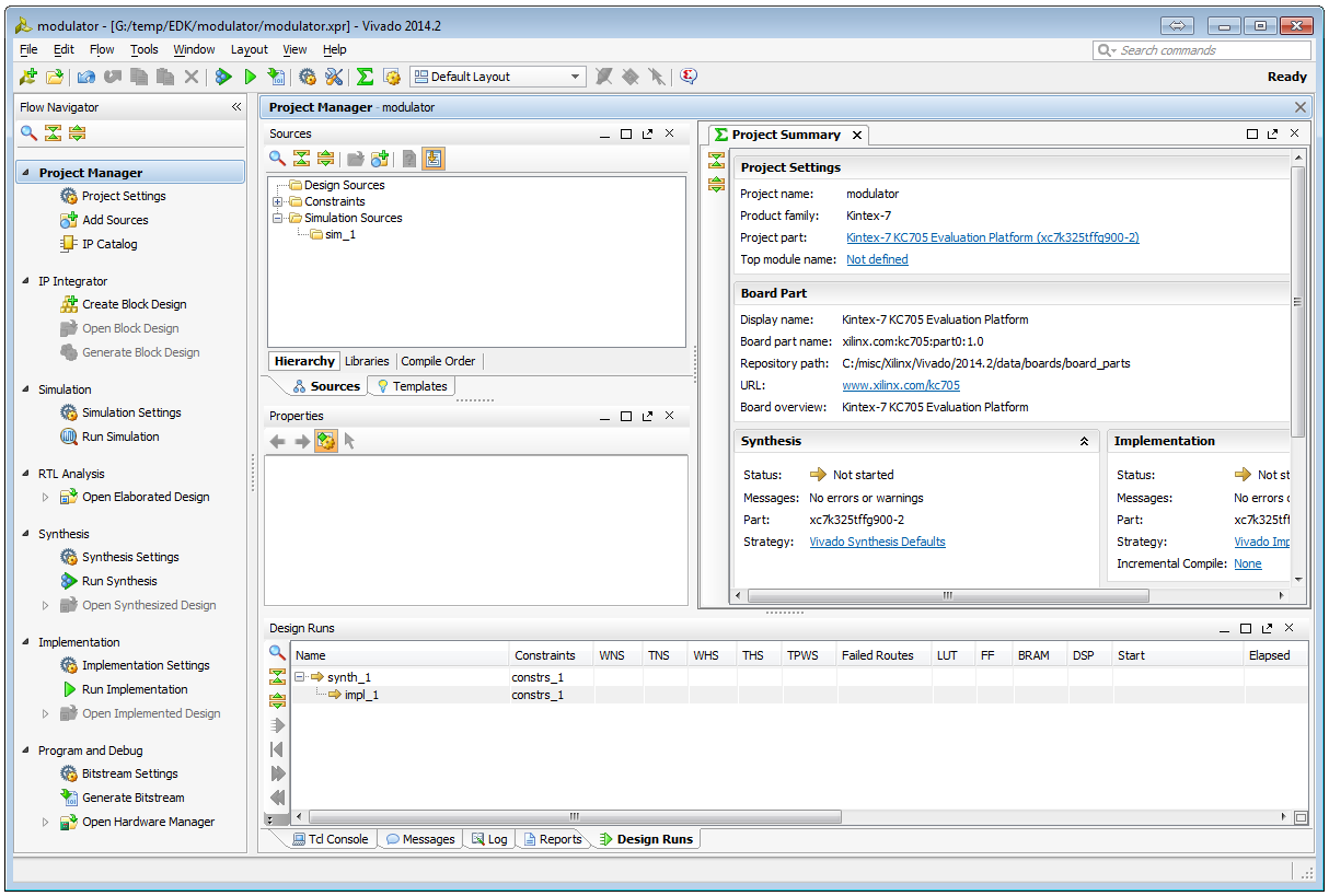
Illustration 2.7: Vivado IDE Viewing Environment
2.2 Vivado Integrated Design Environment
The Vivado IDE can be used for a variety of purposes at various stages in the design flow and is very helpful at detecting design problems early in the design flow.
The Vivado IDE allows different file types to be added as design sources, including Verilog, VHDL, EDIF, NGC format cores, SDC, XDC, and TCL constraints files, and simulation test benches. These files can be stored in variety of ways using the tabs at the bottom of the Sources window: Hierarchy, Library or Compile Order, see Illustration 2.8.
By default, after launching, the Vivado IDE opens the Default Layout. Each docked window in the Vivado IDE is called a view, so you can find Sources View, Properties View, Project Summary View ans so on, see Illustration 2.8.

Illustration 2.8: Vivado IDE Default Layout
Flow Navigator
The vertical toolbar present on the left side of the Vivado IDE is the Flow Navigator. The Flow Navigator provides control over the major design process tasks, such as project configuration, synthesis, implementation and bitstream creation.
Sources View
The Sources view displays the list of source files that has been added in the project.
- The Design Sources folder helps you keep track of VHDL and Verilog design source files and libraries.
- The Constraints folder helps you keep track of the constraints files.
- The Simulation Sources folder helps keep track of VHDL and Verilog simulation sources source files and libraries.
Notice that the design hierarchy is displayed as default.
- In the Libraries tab, sources are grouped by file type, while the Compile Order tab shows the file order used for synthesis.
Project Summary View
The Project Summary view provides a brief overview of the status of different processes executed in the Vivado IDE, see Illustration 2.9.
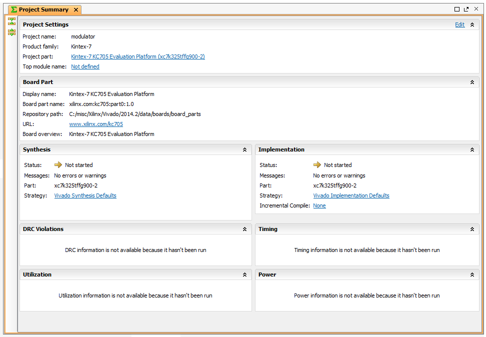
Illustration 2.9: Project Summary View
The Project Settings panel displays the project name, product family, project part, and top module name. Clicking a link in this panel you will open the Project Settings dialog box.
- The Messages panel summarizes the number of errors and warnings encountered during the design process.
- The Synthesis panel summarizes the state of synthesis in the active run. The synthesis panel also shows the target part and the strategy applied in the run.
- The Implementation panel summarizes the state of implementation in the active run. The Implementation panel also shows the target part and the strategy applied in the run.
Tcl Console
Below the Project Summary view, see Illustration 2.8, is the Tcl Console which echoes the Tcl commands as operations are performed. It also provides a means to control the design flow using Tcl commands.
2.3 Create an IP Integrator Design
To accelerate the creation of highly integrated and complex designs, Vivado Design Suite is delivered with IP Integrator (IPI) which provides a new graphical and Tcl-based IP- and system-centric design development flow.
Rapid development of smarter systems requires levels of automation that go beyond RTL-level design. The Vivado IP Integrator accelerates IP- and system-centric design implementation by providing the following:
- Seamless inclusion of IPI sub-systems into the overall design
- Rapid capture and packing of IPI designs for reuse
- Tcl scripting and graphical design
- Rapid simulation and cross-probing between multiple design views
- Support for processor or processor-less designs
- Integration of algorithmic and RTL-level IP
- Combination of DSP, video, analog, embedded, connectivity and logic
- Matches typical designer flows
- Easy to reuse complex sub-systems
- DRCs on complex interface level connections during design assembly
- Recognition and correction of common design errors
- Automatic IP parameter propagation to interconnected IP
- System-level optimizations
The Xilinx Vivado Design Suite IP Integrator feature lets you create complex system designs by instantiating and interconnecting IP cores from the Vivado IP Catalog onto a design canvas.
You can create designs interactively through the IP Integrator design canvas GUI, or using a Tcl programming interface. You will typically construct design at the AXI interface level for greater productivity, but you may also manipulate designs at the port level for more precise design control.
In this tutorial you will instantiate a few IPs in the IP Integrator tool and then stitch them up to create an IP sub-system design. While working on this tutorial, you will be introduced to the IP Integrator GUI, run design rule checks (DRC) on your design, and then integrate the design in a top-level design in the Vivado Design Suite. Finally, you will run synthesis and implementation process, generate bitstream file and run your design on the Kintex-7 KC705 development board.
The following steps describe how to use the IP Integrator within your project:
- In the Flow Navigator, under the IP Integrator and select Create Block Design command, see Illustration 2.10
- In the Create Block Design dialog box, specify a name for your IP subsystem design in the Design name field (in our case it will be modulator), leave Directory field set to the default value of <Local to Project> and click OK, see Illustration 2.11
- The Vivado IDE will display a blank design canvas. You can quickly create complex subsystem by integrating IP cores in it, see Illustration 2.12
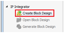
Illustration 2.10: Create Block Design option
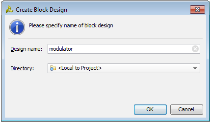
Illustration 2.11: Create Block Design dialog box
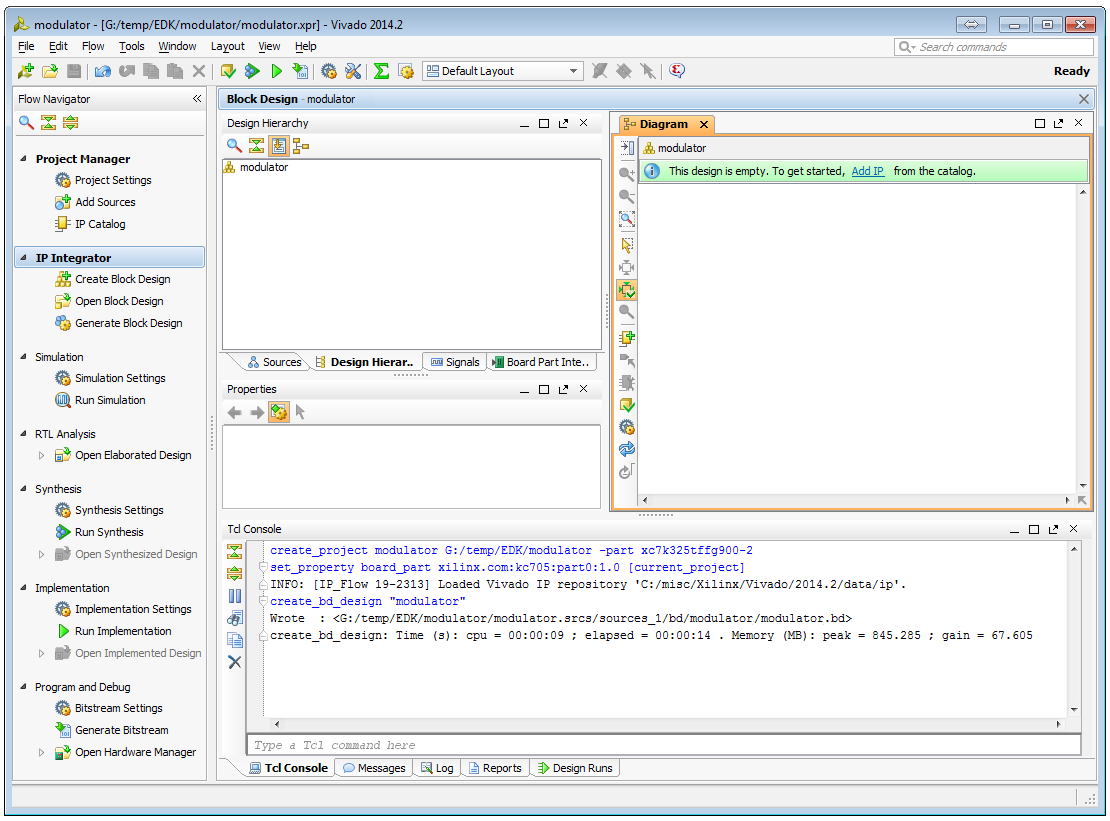
Illustration 2.12: Vivado IDE with a blank design canvas
-
The modulator design is empty. To get started, add IPs from the IP Catalog. You can do that on three ways:
- In the design canvas, right-click and choose Add IP... option, see Illustration 2.13, or
- - Use the Add IP link in the IP Integrator canvas, see Illustration 2.14, or
-
- Click on the Add IP button in the IP Integrator sidebar menu, see Illustration 2.15
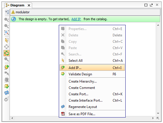
Illustration 2.13: Add IP option
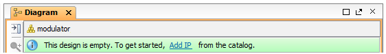
Illustration 2.14: Add IP link
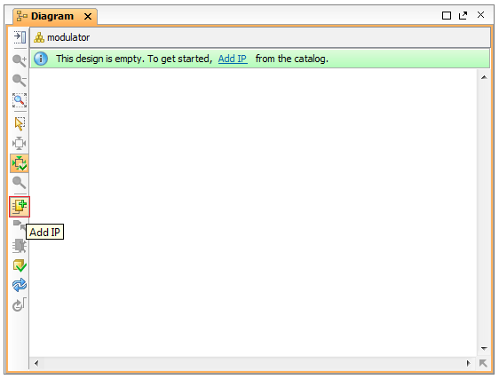
Illustration 2.15: Add IP button
- In the IP Catalog, search for the MicroBlaze core, see Illustration 2.16
- When you find it, press enter on the keyboard or simply double-click on the MicroBlaze (microblaze_0) core in the IP Catalog and the selected core will be automatically instantiated into the IP Integrator design canvas, see Illustration 2.17
-
Right-click in the IP integrator canvas and select the Add IP... option to add the rest of the necessary IPs:
- AXI Timer (axi_timer_0)
- AXI GPIO (axi_gpio_0) to drive the LED
- AXI GPIO (axi_gpio_1) to read the status of the SWITCH
Note: We will not add AXI Interrupt Controller (axi_intc_0) core at this stage of the design. It will be added later as a basic MicroBlaze feature.
- At this point, the IP Integrator canvas should look like as it is shown on the Illustration 2.18
-
In the IP Integrator window, click the Run Block Automation link and select the only supplied /microblaze_0 core, see Illustration 2.19
As you can see from the Illustration 2.19, beside the Run Block Automation link is one more link, Run Connection Automation. Both of the links are IP Integrator features that assist you in putting together a basic microprocessor system, making internal connections between different blocks and making connections to external interfaces.
The Block Automation feature is provided when a microprocessor (such as MicroBlaze processor) is instantiated in the IP Integrator block design. When you click on the Run Block Automation link, you will get assistance with putting together a simple MicroBlaze system.
-
In the Run Block Automation dialog box
- change the Local Memory size from 8 KB to 128 KB
- enable Interrupt Controller
- leave all other parameters unchanged
- As you can see Run Block Automation dialog box allows you to provide input about basic features that the microprocessor system needs, among other things, there is Interrupt Controller core. That was the reason why we didn't add it earlier in the design, in step 6.
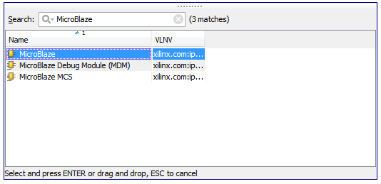
Illustration 2.16: MicroBlaze core in the IP Catalog
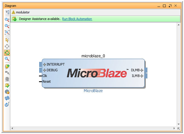
Illustration 2.17: Automatically instantiated MicroBlaze core in the IP Integrator design canvas
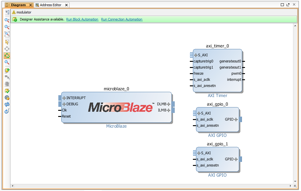
Illustration 2.18: IP Integrator design canvas with all five instantiated IPs
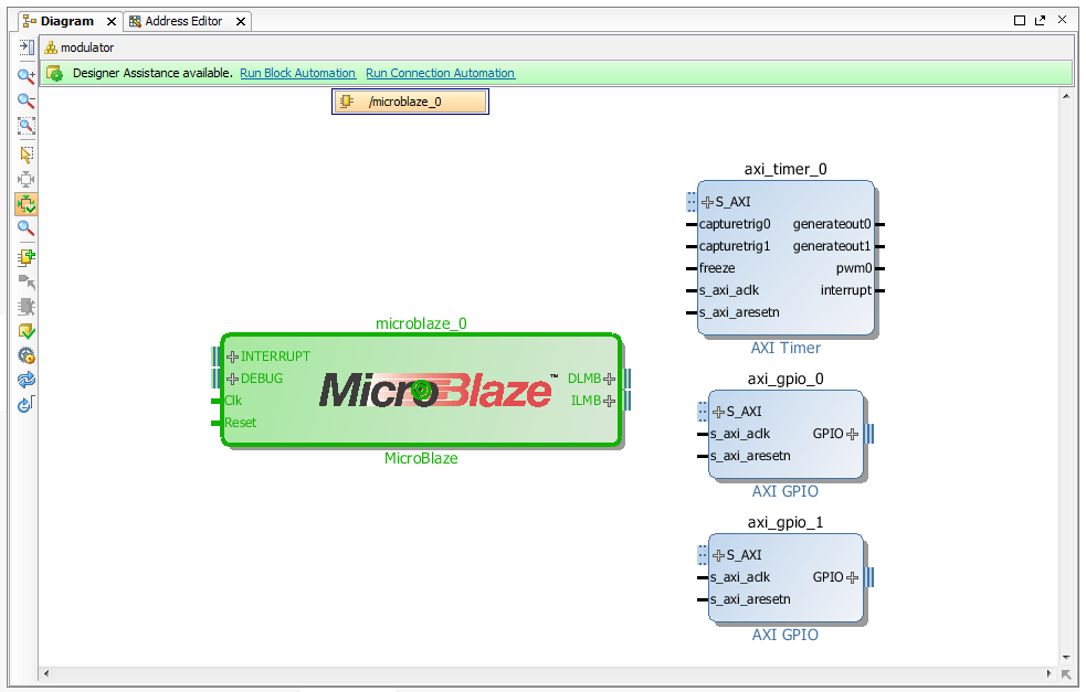
Illustration 2.19: Run Block Automation link
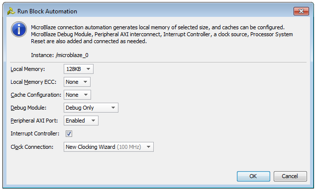
Illustration 2.20: Run Block Automation dialog box
-
When you finished with the Run Block Automation settings, click OK
Ones you specify the necessary options, the Block Automation feature automatically creates a basic system design, see Illustration 2.21
-
In our case, a basic MicroBlaze system consists of:
- mdm_1 block - MicroBlaze Debug Module (MDM)
- microblaze_0_xlconcat block - Concat
- clk_wiz_1 block - Clocking Wizard
- rst_clk_wiz_1_100M block – Processor System Reset
- microblaze_0_local_memory block – a hierarchical block that has the Local Memory Bus, the Local Memory Bus Controller and the Block Memory Generator
- microblalze_0_axi_intc block – AXI Interrupt Controller
- microblaze_0_axi_periph block – AXI Interconnect
Since the design is not connected to any external I/O at this point, IP Integrator tool provides the Connection Automation feature. With this feature you will get assistance in hooking interfaces and/or ports to external I/O ports.
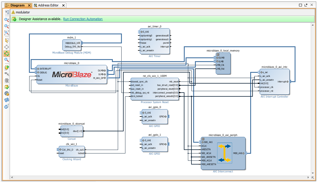
Illustration 2.21: A basic system design created by the Block Automation feature
- In the IP Integrator window, click the Run Connection Automation link and the list of the ports/interfaces that can use the Connection Automation feature will show up, see Illustration 2.22.
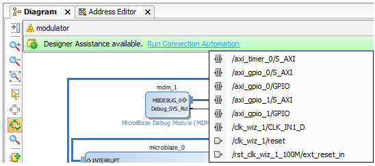
Illustration 2.22: Run Connection Automation link
- As you can see from the illustration above, the design knows the FPGA pins that are connected or used on the target boards. Based on that information, the IP Integrator tool with connection automation feature can assist you in connection the ports in the design to external ports. IP Integrator tool then creates the appropriate physical constraints and other IO constraints required for the IO port in question.
-
Before we use Connection Automation feature, we will change the names of some blocks, in order to make them more descriptive. Change the name of the axi_gpio_0 block to be axi_gpio_LED and axi_gpio_1 to be axi_gpio_SWITCH.
To change the name of some block, do the following:
- Select IP block
- Right-click on it
- Select Block Properties... option
- In the Block Properties dialog box, change the name of the block in the Name field, see Illustration 2.23
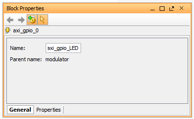
Illustration 2.23: Block Properties dialog box
- - Click Enter
-
Click the Run Connection Automation link and choose the first /axi_timer_0/S_AXI interface. In the Run Connection Automation dialog box leave Auto for Clock Connection and click OK, see Illustration 2.24
This dialog box informs you that the slave AXI port of the GPIO can be connected to the MicroBlaze master. If there are multiple masters in the design, then you will have a choice to select between different masters.
When you click OK in the Run Connection Automation dialog box, the connections will be made and highlighted in the IP Integrator design canvas.
- Repeat the same procedure for /axi_gpio_LED/S_AXI and axi_gpio_SWITCH/S_AXI interfaces
- For /axi_gpio_LED/GPIO interface, in the Run Connection Automation dialog box select led_8bits for Board Part Interface and click OK, see Illustration 2.25
- For /axi_gpio_SWITCH/GPIO interface, in the Run Connection Automation dialog box select dip_switches_4bits for Board Part Interface and click OK
- For /clk_wiz_1/CLK_IN1_D interface, in the Run Connection Automation dialog box leave sys_diff_clock for Board Part Interface and click OK
- For /clk_wiz_1/reset port, in the Run Connection Automation dialog box leave reset for Board Part Interface and click OK
- For /rst_clk_wiz_1_100M/ext_reset_in port, in the Run Connection Automation dialog box leave reset for Board Part Interface and click OK
-
First, remove microblaze_0_xlconcat block from the IP Integrator design canvas, because in our design there is only one interrupt source (axi_timer_0)
To remove block from the IP Integrator design canvas, it is enough to select desired block and click Delete button on your keyboard
-
Connect the interrupt port of the axi_timer_0 block to the intr[0:0] port of the microblaze_0_axi_intc block
Place the cursor on top of the desired pin and you can notice that the cursor changes into a pencil indicating that a connection can be made from that pin. Clicking the left mouse button a connection starts. Click and drag the cursor from one pin to another. You must press and hold down the left mouse button while dragging the connection from one pin to another. As you drag the connection wire, a green checkmark appears on the port indicating that a valid connection can be made between these points. The Vivado IP Integrator highlights all possible connections points in the subsystem design as you interactively wire the pins and ports. Release the left mouse button and Vivado IP integrator makes connection between desired ports. Repeat this procedure until all the pins become associated.
- Right-click in the IP integrator canvas and select the Add IP... option to add the last IP block necessary for our design. Search for the Constant (xlconstant_0) core and add it into our design.
-
Double-click on the Constant block and set the constant value, Const Val, to be 0 and click OK, see Illustration 2.26.
This step is important because we have to connect the unconnected input ports of the AXI Timer (axi_timer_0) block (capturetrig0, capturetrig1 and freeze) to GND, because we won't need them in our design. Using the Constant block is one possible way how to solve this problem.
- Connect the capturetrig0, capturetrig1 and freeze ports of the AXI Timer (axi_timer_0) block to the dout[0:0] port of the new Constant (xlconstnt_0) block
- Also connect the aux_reset_in port of the Processor System Reset (rst_clk_wiz_1_100M) to the dout[0:0] port of the Constant (xlconstnt_0) block
- Leave generateout0, generateout1 and pwm output ports of the AXI Timer (axi_timer_0) block unconnected
-
From the sidebar menu of the design canvas, run the IP subsystem design rule checks by clicking the Validate Design button
Alternatively, you can do the same by selecting Tools → Validate Design from the main menu, see Illustration 2.28, or
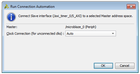
Illustration 2.24: Run Connection Automation dialog box for /axi_timer_0/S_AXI interface
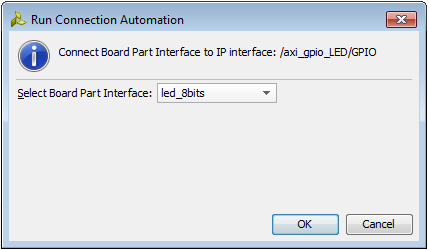
Illustration 2.25: Run Connection Automation dialog box for /axi_gpio_LED/GPIO interface
Now, when we have connected all the ports/interfaces offered by the Connection Automation wizard, we will manually connect the rest of the ports/interfaces
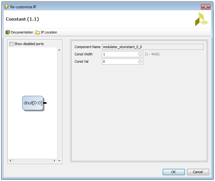
Illustration 2.26: Re-customize IP dialog box for Constant IP block

Illustration 2.27: Finial Block Diagram of our design
When we have connected all the necessary ports/interfaces in our design, see Illustration 2.27, it is time to validate it.
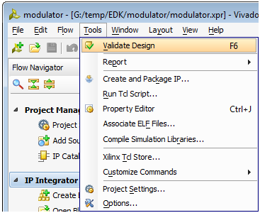
Illustration 2.28: Validate Design option from the main menu
- by clicking the design canvas and selecting Validate Design button from the main toolbar menu, see Illustration 2.29
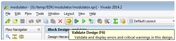
Illustration 2.29: Validate Design button from the main toolbar menu
- ln the Validate Design dialog box, click OK, see Illustration 2.30
- At this point, you should save the IP integrator design. Use the File → Save Block Design command from the main menu to save the design.
- In the Vivado Flow Navigator, under the Project Manager, click on the Project Settings command and in the Project Settings dialog box check is the Target language set to VHDL. If it is not, please change it to be VHDL, see Illustration 2.31.
- In the Sources window, select modulator, right-click on it and choose Create HDL Wrapper... option, see Illustration 2.32
- In the Create HDL Wrapper dialog box, select Let Vivado manage wrapper and auto-update option and click OK, see Illustration 2.33
- After the HDL wrapper is generated, you should see it in the Sources window, see Illustration 2.34
-
In the Vivado Flow Navigator, click Run Synthesis command (Synthesis option) and wait for task to be completed
Note: You can monitor the Synthesis progress in the bar in the upper-right corner of the Vivado IDE.
- After the synthesis is completed, the Synthesis Completed dialog box will appear. Select Open Synthesized Design and click OK
-
The last step in our hardware design will be to crate and add modulator_mb.xdc constraints file. To create a XDC file using the Vivado IDE GUI, do the following:
-
Change the layout from the Default Layout to I/O Planning view, in the layout pull-down menu in the main toolbar, to identify pins that don't have an assigned location, see Illustration 2.35
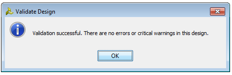
Illustration 2.30: Validate Design dialog box
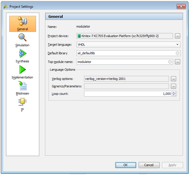
Illustration 2.31: Project settings dialog box
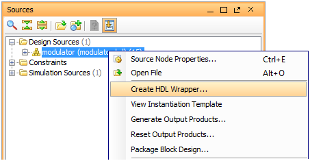
Illustration 2.32: Create HDL Wrapper option
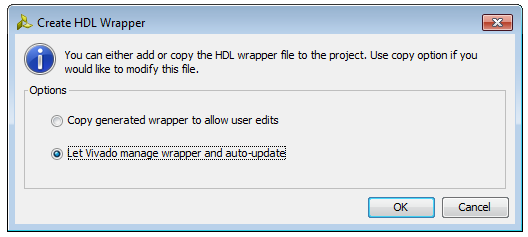
Illustration 2.33: Create HDL Wrapper dialog box
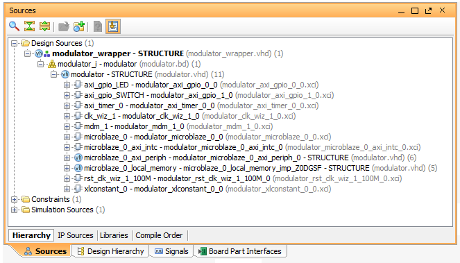
Illustration 2.34: Sources window with generated HDL wrapper
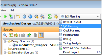
Illustration 2.35: IO Planning layout
- This will change the layout from the Default view to the I/O Planning view, see Illustration 2.36
- The main window of the I/O Planning view displays the package view of the Kintex-7 device. Below the Package view, two additional tabs are populated. One tab displays the list of I/O ports of the design and the second tab displays the list of package pins on the device package.
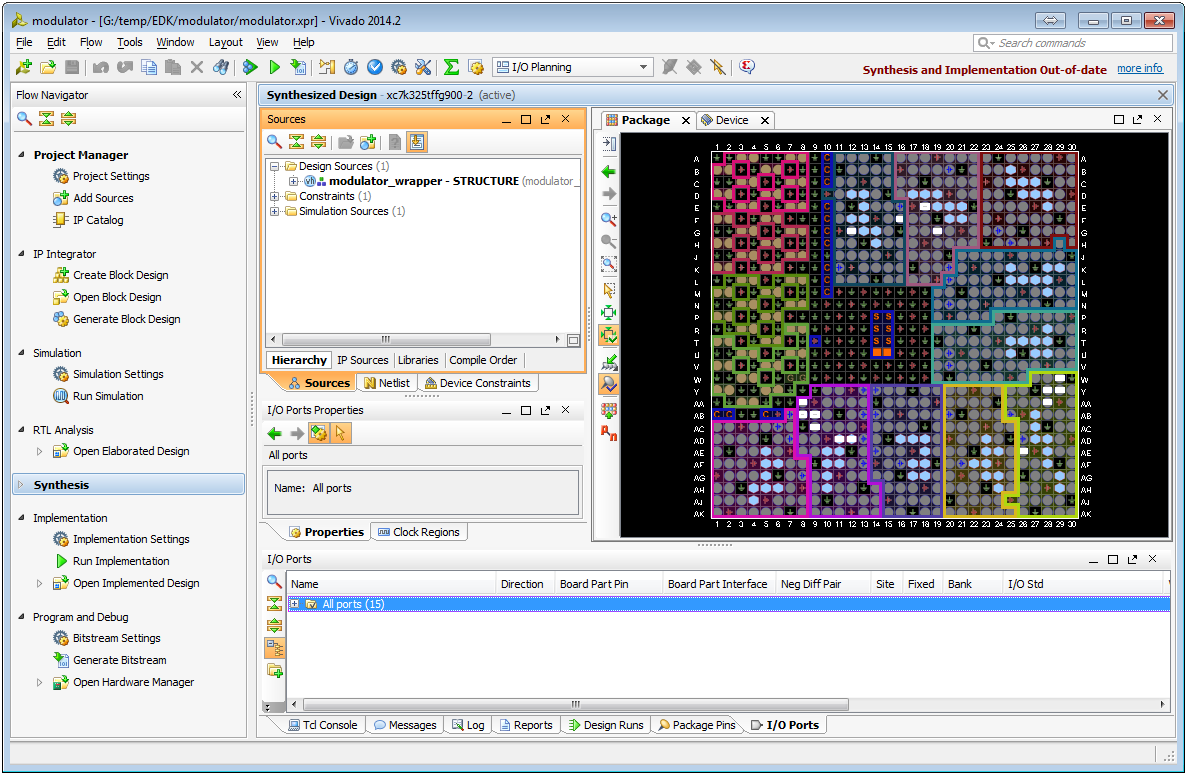
Illustration 2.36: I/O Planning View
-
In the I/O Ports tab, click Expand All option, or just expand All ports, which shows all I/O Ports of your design
Grey icons indicate unplaced ports, while yellow icons indicate placed ports. After we assign a pin location to each of the I/O ports they will be colored yellow, as can be seen on the Illustration 2.38.
-
To connect your logical with your physical ports, select one scalar port (for example reset) and find in the user guide for the Kintex-7 (KC705) evaluation board to which pin location you would like to connect your reset port. In our case it will be:
set_property PACKAGE_PIN G12 [get_ports GPIO_SW_C]
set_property IOSTANDARD LVCMOS25 [get_ports GPIO_SW_C]
- Click on the reset's Site column and choose G12 as a pin location to connect the reset port
- Click on the reset's I/O Std column and change the I/O standard to be LVCMOS25
-
Leave all the other reset's options unchanged, because they are default values
Note: After assigning pin location and I/O standard for reset port, we can notice that I/O Port Properties window popped up. This is the another way to change port properties, see Illustration 2.37. If you want to apply some changes that you made, just click the Automatically update button.
-
Repeat these configuration steps for the remaining ports using the port map information below:
set_property PACKAGE_PIN F16 [get_ports GPIO_LED_7_LS]
set_property IOSTANDARD LVCMOS25 [get_ports GPIO_LED_7_LS]
set_property PACKAGE_PIN E18 [get_ports GPIO_LED_6_LS]
set_property IOSTANDARD LVCMOS25 [get_ports GPIO_LED_6_LS]
set_property PACKAGE_PIN G19 [get_ports GPIO_LED_5_LS]
set_property IOSTANDARD LVCMOS25 [get_ports GPIO_LED_5_LS]
set_property PACKAGE_PIN AE26 [get_ports GPIO_LED_4_LS]
set_property IOSTANDARD LVCMOS25 [get_ports GPIO_LED_4_LS]
set_property PACKAGE_PIN AB9 [get_ports GPIO_LED_3_LS]
set_property IOSTANDARD LVCMOS15 [get_ports GPIO_LED_3_LS]
set_property PACKAGE_PIN AC9 [get_ports GPIO_LED_2_LS]
set_property IOSTANDARD LVCMOS15 [get_ports GPIO_LED_2_LS]
set_property PACKAGE_PIN AA8 [get_ports GPIO_LED_1_LS]
set_property IOSTANDARD LVCMOS15 [get_ports GPIO_LED_1_LS]
set_property PACKAGE_PIN AB8 [get_ports GPIO_LED_0_LS]
set_property IOSTANDARD LVCMOS15 [get_ports GPIO_LED_0_LS]
set_property PACKAGE_PIN Y28 [get_ports GPIO_DIP_SW3]
set_property IOSTANDARD LVCMOS25 [get_ports GPIO_DIP_SW3]
set_property PACKAGE_PIN AA28 [get_ports GPIO_DIP_SW2]
set_property IOSTANDARD LVCMOS25 [get_ports GPIO_DIP_SW2]
set_property PACKAGE_PIN W29 [get_ports GPIO_DIP_SW1]
set_property IOSTANDARD LVCMOS25 [get_ports GPIO_DIP_SW1]
set_property PACKAGE_PIN Y29 [get_ports GPIO_DIP_SW0]
set_property IOSTANDARD LVCMOS25 [get_ports GPIO_DIP_SW0]
set_property PACKAGE_PIN AD12 [get_ports SYSCLK_P]
set_property IOSTANDARD LVDS [get_ports SYSCLK_P]
- When you are finished with the placement constraints, click File → Save Constraints As...
- In the Save Constraints As dialog box, type the name of the constraint set in the New Constraints set name field. In our case, the name will be modulator_mb.
- Click OK and your modulator_mb.xdc constraint file should appear in the Sources window under the Constraints, see Illustration 2.39
- In the Vivado Flow Navigator, click Run Synthesis command, see Illustration 2.40, and wait for task to be completed
- When the synthesis process is completed, click Run Implementation command, see Illustration 2.40, and wait for task to be completed
-
At the end, when the implementation process is completed, click Generate Bitstream command, see Illustration 2.40
After this step, bitstream file will be generated.
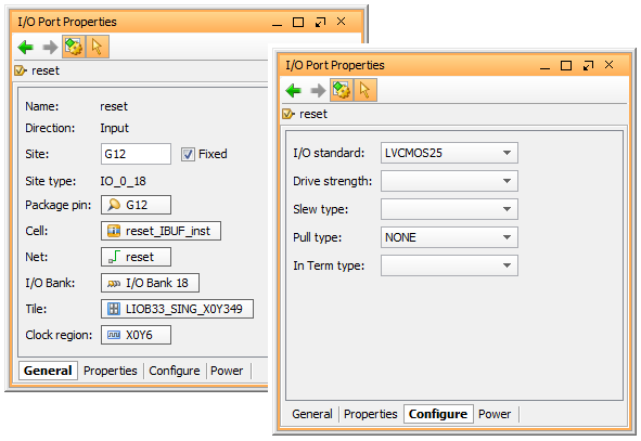
Illustration 2.37: I/O Port Properties window
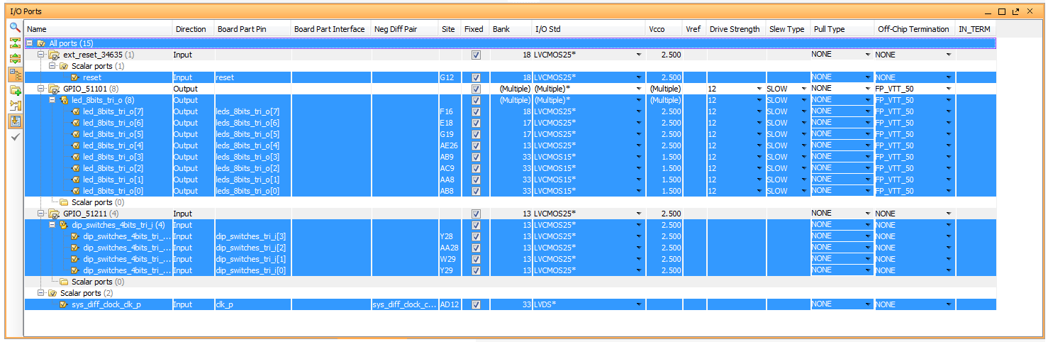
Illustration 2.38: I/O Ports tab with assigned pin locations and I/O standards
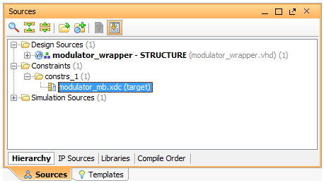
Illustration 2.39: Created modulator_mb constraints file in the Sources window
To prepare our design to work in the FPGA device, we must convert it to a bitstream file. This process is composed of two important steps. One is to generate a netlist file that will represent your hardware platform and the second one is to generate a bitstream file that will represent the hardware and software platforms together. This bitstream file will be downloaded to the FPGA device.
There are two possibilities for netlist and bitstream file generation. One is to generate these files after a hardware platform is specified and the second one is to generate them after a software application development is completed.
If you would you like to generate netlist and bitstream file after hardware platform specification:
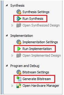
Illustration 2.40: Run Synthesis, Run Implementation and Generate Bitstream commands from the Vivado Flow Navigator
If you would you like to generate netlist and bitstream files after a software application development is completed, please follow the next chapter where will be explained in detail the necessary steps.