4. DEBUGGING SYSTEM USING VIVADO LOGIC ANALYZER
Vivado Logic Analyzer is an integrated logic analyzer in the Vivado Design Suite. In this chapter you will learn how to debug your MicroBlaze-based system using the Vivado logic analyzer and you will take advantage of it's functions to debug and discover some potential root causes of your design.
In-system debugging allows you to debug your design in real-time on your target hardware. IP Integrator provides ways to instrument your design for debugging, which will be explained in this chapter. There are two flows (methods) supported in the Vivado Debug Probing:
-
HDL Instantiation Debug Probing Flow
This flow involves the manual customizations, instantiation, and connection of various debug core components directly in the HDL design source. Debug cores that are supported in this flow, in the Vivado tool, are:
- Integrated Logic Analyzer (ILA) core v4.0
- Virtual Input/Output (VIO) core v3.0
- Integrated Bit Error Ratio Tester (IBERT) core v3.0
- JTAG to AXI Master core v1.0
-
Using the Netlist Insertion Debug Probing Flow
Insertion of debug cores in the Vivado tool is presented in a layered approach to address different needs of the diverse group of Vivado users:
- The highest level is a simple wizard that creates and configures Integrated Logic Analyzer (ILA) cores aurtomatically based on the selected set of nets to debug
- The next level is the main Debug window allowing control over individual debug cores, ports and their properties
- The lowest level is the set of Tcl debug commands that you can enter manually or replay as a script
What is also important to note is that you can use combination of the modes to insert and customize debug cores
Choosing the flow depends on your preferences and types of nets/signals that you are interested in debugging. In this tutorial we will explain the Netlist Insertion Debug Probing Flow on the Modulator IP integrated design.
In this flow you will mark nets that you are interested in analyzing in the block design. Marking nets for debug in the block design offers more control in terms of identifying debug signals during coding and enabling/disabling debugging later in the flow.
To start debugging process using the Netlist Insertion Flow in IP Integrator tool, please do the following:
- In the Vivado IDE Flow Navigator, click on the Open Block Design command under the IP Integrator to open our modulator block design, see Illustration 4.1
-
The next step will be to mark nets for debug
Nets can be marked for debug in the block design by highlighting them, right-clicking on them and selecting Mark Debug option, see Illustration 4.2
-
Mark the following nets for debug:
- in the microblaze_0_local_memory IP - DLMB interface
- in the axi_gpio_LED IP - S-AXI interface and GPIO bus
The nets that have been marked for debug will show a small bug icon placed on top of the net in the block design. Likewise, a bug icon can be seen placed on the nets to be debugged in the Design Hierarchy window as well.
- The next step is to synthesize the design by clicking on the Run Synthesis command from the Flow Navigator, under the Synthesis drop-down list
- In the Synthesis Completed dialog box, select Open Synthesized Design option and click OK
- The Schematic and the Debug window opens
- In the Debug window, click on the Set Up Debug icon, see Illustration 4.3, to launch Set Up Debug wizard to guide you through the process of automatically creating debug cores and assigning debug nets to the inputs of the cores

Illustration 4.1: Finial Block Diagram of our design
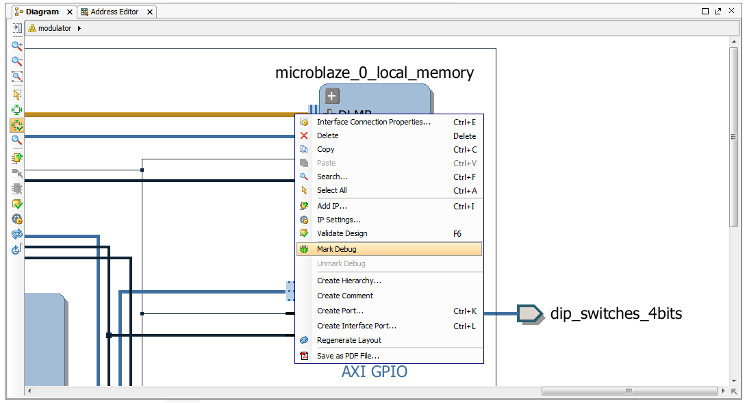
Illustration 4.2: Mark Debug option
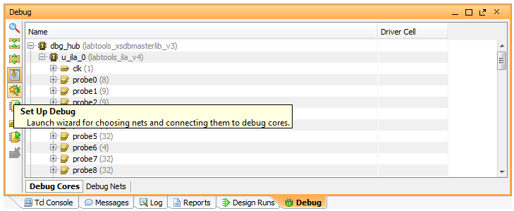
Illustration 4.3: Set Up Debug button
The another way to launch this wizard is to select Tools → Set up Debug... option from the Vivado IDE main menu, see Illustration 4.4
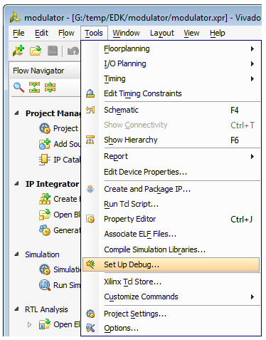
Illustration 4.4: Tools → Set up Debug option
- In the Set Up Debug dialog box, click Next
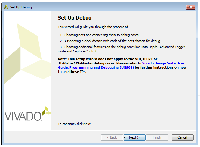
Illustration 4.5: Set Up Debug dialog box
- In the Existing Debug Nets dialog box, choose how to handle existing nets connected to debug cores. Leave selected Continue debugging 176 nets connected to existing debug core option, as it is shown on the Illustration 4.6, and click Next
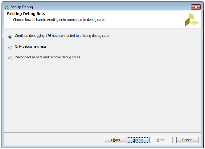
Illustration 4.6: Existing Debug Nets dialog box
- In the Additional Debug Nets dialog box, choose additional 39 unassigned debug nets to debug and click Next
- In the Specify Nets to Debug dialog box you will find nets that you have marked for debugging, see Illustration 4.8
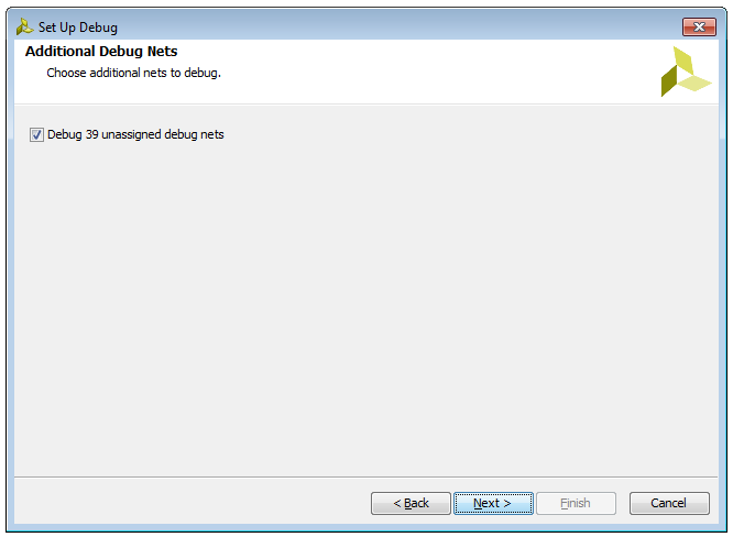
Illustration 4.7: Additional Debug Nets dialog box
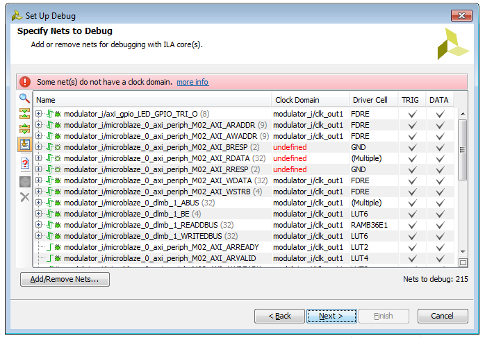
Illustration 4.8: Specify Nets to Debug dialog box
- In the Specify Nets to Debug dialog box, you have also an opportunity to add more nets or remove existing nets from the table. Click Add/Remove Nets... button to open Add/Remove Nets dialog box, see Illustration 4.8
-
In the Add/Remove Nets dialog box, select the net in the Nets to Debug (176) window and click on the arrow to remove the net from the debug nets list, see Illustration 4.9.
Remove all the nets with undefined clock domain. In our case it will be six nets, see Illustration 4.9.
- If you are satisfied with the debug net selection, click OK
- In the Specify Nets to Debug dialog box you can see that nets that are removed in the Add/Remove Nets dialog box are not existing anymore in the list of nets prepared for debugging with ILA core, see Illustration 4.10.
- Note that all nets belong to the same clock domain, because signals captured by the same ILA core must have the same clock domain.
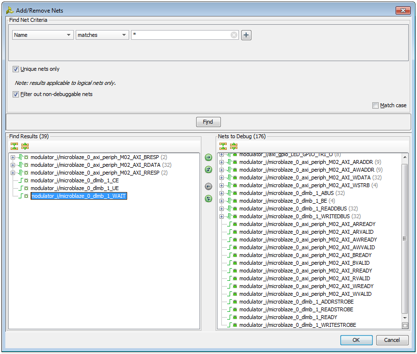
Illustration 4.9: Add/Remove Nets dialog box
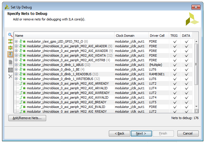
Illustration 4.10: Specify Nets to Debug dialog box
- Ones you are satisfied with the debug net selection, click Next
-
In the ILA (Integrated Logic Analyzer) General Options dialog box:
- change the Sample of Data Depth value to 8192
- leave Input Pipe Stages to be 0
- enable Capture Control and Advanced Trigger options in the Trigger and Storage Settings, see Illustration 4.11
- click Next
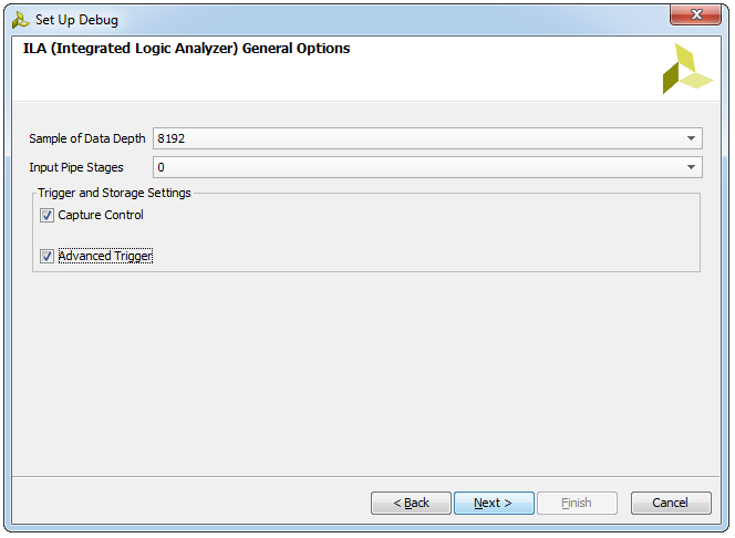
Illustration 4.11: ILA General Options dialog box
Important: The Set up Debug wizard inserts one ILA core per clock domain!
The nets that were selected for debug are assigned automatically to the probe ports of the inserted ILA v4.0 core. The last wizard screen shows the core creation summary displaying the number of clocks found and ILA cores to be created and/or removed, see Illustration 4.12
- If you are satisfied with the results, click Finish in the Set Up Debug Summary dialog box to insert and connect the ILA v4.0 core in your synthesized design netlist, see Illustration 4.12
- The debug nets are now assigned to the ILA v4.0 debug core, what you can see in the Debug window, see Illustration 4.13
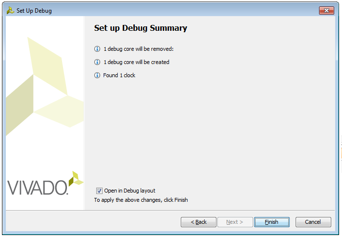
Illustration 4.12: Set Up Debug Summary dialog box
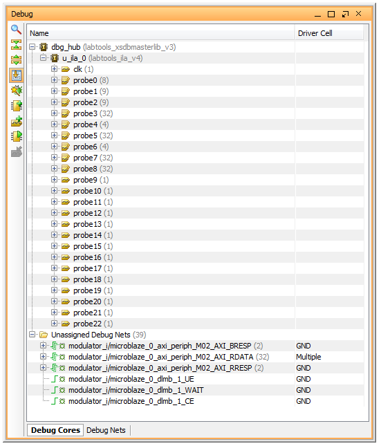
Illustration 4.13: Debug window with assigned debug nets
- The generated ILA core you can also find in the Netlist window, see Illustration 4.14
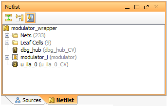
Illustration 4.14: Netlist window with generated ILA core
Now when debug nets are assigned to the ILA debug core, we must re-implement our design and re-generate new bitstream file.
- In the Vivado Flow Navigator, click Run Implementation command, see Illustration 4.15, and wait for task to be completed
-
When the implementation process is completed, click Generate Bitstream command, see Illustration 4.15, and wait for task to be completed
After this step, bitstream file will be generated.
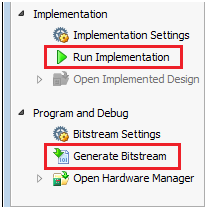
Illustration 4.15: Run Implementation and Generate Bitstream options
- Select File → Export → Export Hardware option from the main Vivado IDE menu
- In the Export Hardware dialog box, make sure that Include bitstream check box is checked, and Export to field is set to <Local to Project> and click OK
- Select File → Launch SDK from the main Vivado IDE menu to launch SDK after the hardware platform has been exported
- In the Launch SDK dialog box, make sure that both Exported location and Workspace set to <Local to Project> and click OK
-
To download your new bitstream file to the target board, select Xilinx Tools → Program FPGA from the SDK main window
-
In the Program FPGA dialog box:
- For Hardware Configuration:
- set Hardware Platform to be modulator_wrapper_hw_platform_0
- set Connection to be Local
- For Software Configuration:
- choose in the EFF File to Initialize in Block RAM drop-down many new modulator_no_intc.elf file, see Illustration 4.16
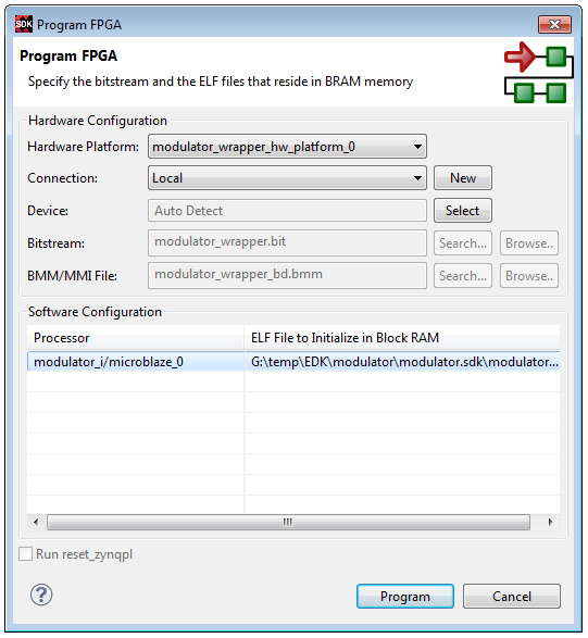
Illustration 4.16: Program FPGA dialog box
-
Click Program and your updated bitstream file with the .elf file will be downloaded into the target FPGA device
4.1 Illustration of using Vivado Logic Analyzer tool
Ones you have the debug cores in your design, you can use the logic analyzer to debug the design in hardware.
To access the Vivado logic analyzer feature:
- In the Vivado Flow Navigator, click the Open Hardware Manager command in the Program and Debug section, see Illustration 4.17
- After programming the FPGA device with the .bit file that contains the ILA v4.0 core, the Hardware window now shows the ILA core that were detected after scanning the device, see Illustration 4.18
- The next step in design debugging process is to set up the ILA core. Click on the ILA core (called hw_ila_1 core) in the Hardware window and then click on the “Open ILA Dashboard” link in the ILA Core Properties window to see its properties in the ILA Properties window, see Illustration 4.19
- First we will use the ILA core to capture the AXI data write transaction to the axi_gpio_LED component. GPIO port of the axi_gpio_LED component is connected to the LEDs, present on the development board, so to turn on and off the LED we must write the appropriate values into the register that is part of the axi_gpio_LED component. This is done using the AXI interface that connects the axi_gpio_LED component to the MicroBlaze processor. In order to capture the AXI data write transaction to the axi_gpio_LED component, ILA core must be setup in the following way. We will setup the ILA core to trigger when a LED is turned on. This means that the value 0x80 will be written into the axi_gpio_LED component. To capture this condition, we must use advanced trigger mode of ILA core. In the ILA Properties window, select ADVANCED_ONLY option from the Trigger mode drop-down list, like it is shown on the Illustration 4.20
- ILA core will now use advanced triggering mode allowing us to specify a sequence of events that must occur in order to trigger the ILA core. To specify trigger sequence we must create a new trigger state machine by selecting Create new trigger state machine option in the Trigger State Machine window, like it is show on the Illustration 4.22. At this time we can also set Trigger position in window value to 4000, which is also show on the Illustration 4.21.
- Ones you click on the Create new trigger state machine option a window will appear, asking you to specify the new trigger state machine file name and its location. Name the new trigger state machine file as Trigger_FSM1 and save it.
- After you have created Trigger_FSM1 state machine file its current content will be shown in the Trigger State Machine window. We must modify this content, as shown on the Illustration 4.22.
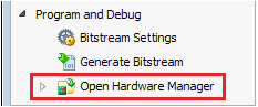
Illustration 4.17: Open Hardware Manager command
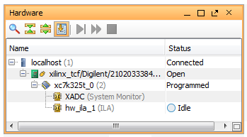
Illustration 4.18: Hardware window showing the ILA core
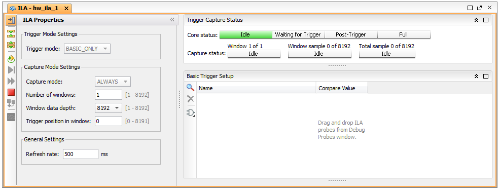
Illustration 4.19: ILA Properties window
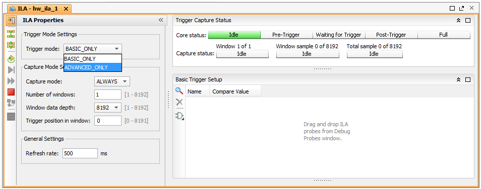
Illustration 4.20: Selecting ADVANCED_ONLY trigger mode
Illustration 4.21: Create new trigger state machine
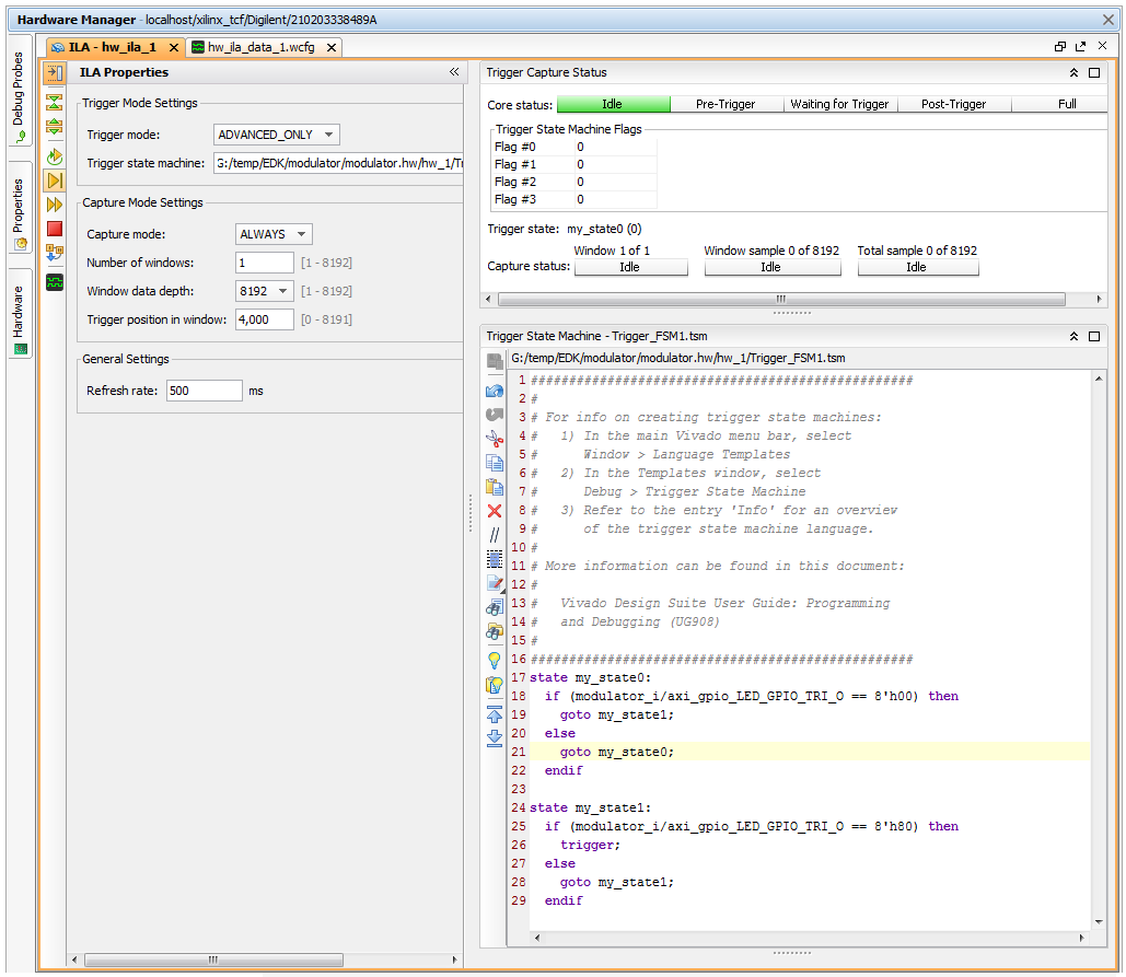
Illustration 4.22: Trigger FSM code
- Our trigger state machine consists from two states, my_state0 and my_state1, as shown on the Illustration 4.23. Initially, trigger state machine is in the my_state0 state, waiting until axi_gpio_LED__GPIO_TRI_O probe has the value of 0x00. When this condition is met, trigger state machine transitions to my_state1 state. While in this state, trigger state machine waits until axi_gpio_LED__GPIO_TRI_O probe has the value of 0x80. When this condition is met, trigger state machine will trigger the ILA core and sample and store the ILA probe signals.
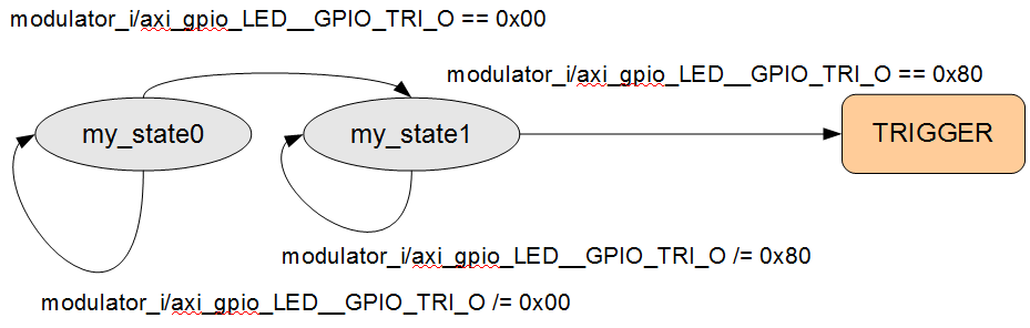
Illustration 4.23: Trigger FSM State Diagram
- Having defined trigger sequence, we can arm the ILA core by clicking on the Run Trigger button .
-
Once the ILA core captured data has been uploaded to the Vivado IDE, it is displayed in the Waveform Viewer. Use the Zoom In button to zoom-in into the area around the trigger marker, shown as the vertical red line, in order to see waveforms of different signals and buses that are part of the AXI interface, as shown on the Illustration 4.24.
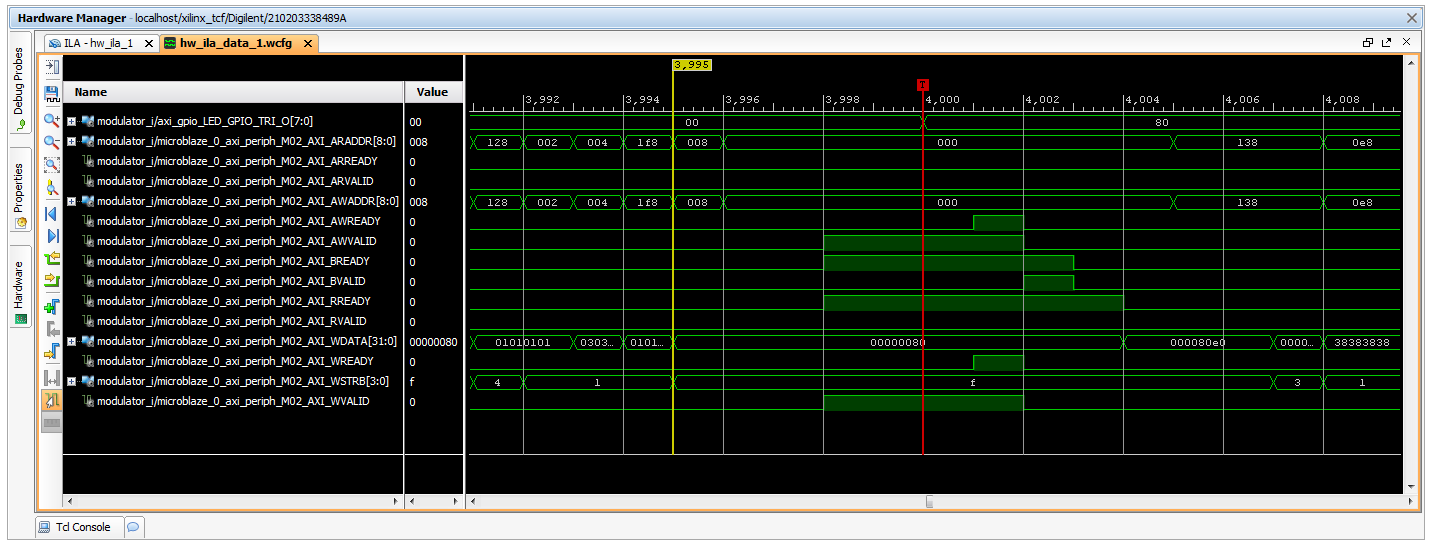
Illustration 4.24: Captured waveform after trigger condition is reached
-
From the Illustration 4.24 we can see that the ILA has triggered exactly on the transition that we have specified in our trigger state machine code. Trigger marker is positioned exactly on the point where axi_gpio_LED__GPIO_TRI_O probe transitions from value 0x00 to value 0x80. ILA has stored 4000 samples before this condition and additional 4192 samples after this condition in its buffer, exactly as was specified. Furthermore, from the captured waveform we can also see the AXI interface data write sequence. Value of 0x00000080 is placed on the microblaze_0_axi_periph_M02_AXI_WDATA write data bus while the microblaze_0_axi_periph_M02_AXI_AWADDR write address bus has the value of 0x000. This is the address of the Channel1 AXI GPIO Data Register from the axi_gpio_LED component that is connected to the LEDs on the development boards, please see Table 2-4, on page 9, in the “PG144 LogiCORE AXI GPIO v2.0 Product Guide”.
Data is actually written into this register when microblaze_0_axi_periph_M02_AXI_WSTRB bus is set to value of 0xf and microblaze_0_axi_periph_M02_AXI_WREADY signal goes high.
4.2 Illustration of using Vivado Logic Analyzer together with SDK Debugger
In the previous sub-chapter we have shown in one example how you can use Vivado Logic Analyzer to debug MicroBlaze-based system. Now we will show in one another example how you can use Vivado Logic Analyzer together with SDK debugger tool to debug your design.
- Our first step will be to remove all the Breakpoints added in our design in the previous sub-chapters. To remove breakpoints from our design, in the SDK open Breakpoints tab, select breakpoints that you want to remove, right-click on them and select Remove option, see Illustration 4.25.
- When we removed all unnecessary breakpoints from our design, we will now add new breakpoint, at line 101, see Illustration 4.26. This breakpoint will stop program execution at the moment of sine_ampl array initialization. We can use the Vivado Logic Analyzer to overview this initialization process directly in hardware, by monitoring the DLMB memory interface that connects the MicroBlaze processor with the on-chip memory sub-system where sine_ampl array will be stored.
- In the Properties for C/C++ Line Breakpoint dialog box, leave all parameters unchanged and click OK, see Illustration 4.27
- In the SDK, click Resume button in order to execute program until a breakpoint at line 101 is reached
- Turn back to the Vivado IDE, to the Hardware Manager and in the ILA Properties window set ILA Trigger mode to BASIC_ONLY, see Illustration 4.29
- The next step will be to decide what ILA debug probes are required to participate in the trigger condition. Go to the Debug Probes window, select the desired ILA debug probes (microblaze_0_dlmb_1_ABUS[3:31] and microblaze_0_dlmb_1_WRITESTROBE), right-click on them and select Add Probes to Basic Trigger Setup option, see Illustration 4.28.
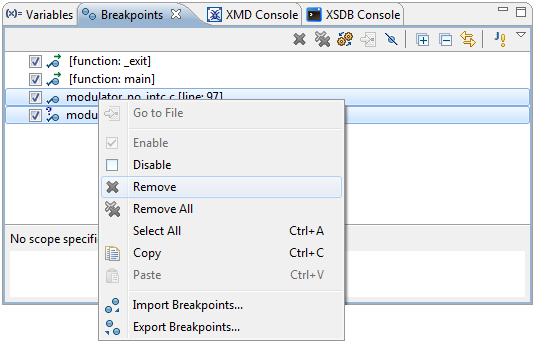
Illustration 4.25: Breakpoint tab – Remove option
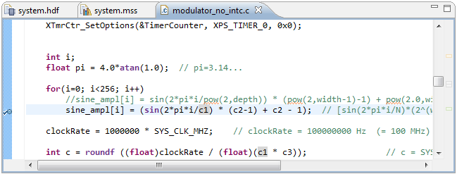
Illustration 4.26: Added Breakpoint at line 101
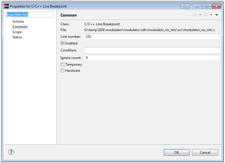
Illustration 4.27: Properties for C/C++ Line Breakpoint dialog box
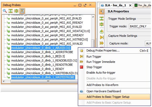
Illustration 4.28: Add Probes to Basic Trigger Setup option
- The another way to add debug probes to the Basic Trigger Setup window is to drag and drop the probes from the Debug Probes window to the Basic Trigger Setup window.
Important: Only probes that are in the Basic Trigger Setup window participate in the trigger condition. Any probes that are not in the window are set to “don't care” values and are not used as part of the trigger condition.
- Note: If you want to remove probes from the Basic Trigger Setup window, select the probe, right-click on it and choose Remove option.
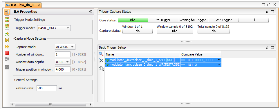
Illustration 4.29: Added probes to the ILA Basic Trigger Setup window
- Now, when the ILA debug probes microblaze_0_dlmb_1_ABUS[3:31] and microblaze_0_dlmb_1_WRITESTROBE are in the Basic Trigger Setup window, see Illustration 4.29, we can create trigger condition and debug probe compare values.
- In the Basic Trigger Setup window, select the Compare Value cell for the microblaze_0_dlmb_1_ABUS[3:31] ILA debug probe to open the Compare Value dialog box, see Illustration 4.30
- In the Compare Value dialog box, set the Value to be 0000_9350 as it is shown on the Illustration 4.30, because this is the address of the first element in the sine_ampl array. Please refer to step 12 in the Sub-chapter 3.7.3 Debug Perspective for the explanation how to find out the starting address of the sine_ampl array. Click OK.
- Repeat the same procedure for microblaze_0_dlmb_1_WRITESTROBE probe. Select the Compare Value cell of the microblaze_0_dlmb_1_ WRITESTROBE ILA debug probe and in the Compare Value dialog box set the Value to be 1, see Illustration 4.31. This probe is needed in order to trigger ILA core in the moment when data is being written into the memory location with address 0x9350. Click OK.
- After we set all the ILA core parameters, we can arm the ILA core. Click the Run Trigger button
- After we arm the ILA core, in the ILA Properties window you can see the ILA Trigger Capture Status, see Illustration 4.32. You can see that the ILA Core status is “Waiting for Trigger”, because the triggering condition hasn't been met yet. Capture status shows that 4000 samples have already been stored in the ILA core buffer and the remaining 4192 samples will be stored when the trigger condition is met. This is because we have specified Trigger position in window to be 4000 samples.
- Go back to the SDK and click Step Over command to execute the line 101
- Ones the ILA core captured data has been uploaded to the Vivado IDE, it is displayed in the Waveform Viewer. Open the waveform viewer and remove all the signals that are present.
- Go to the Debug Probes window and add all the probes connected to the DLMB interface (there should be 8 probes). Select all the probes connected to the DLMB interface, right-click on them and select Add Probes to Waveform option, see Illustration 4.33.
- In the Waveform Viewer you should see all the probes connected to the DLMB interface, see Illustration 4.34. Press Zoom In button several times to zoom-in into the area around the trigger marker, shown as the vertical red line, in order to see waveforms of different signals and buses that are part of the DLMB interface.
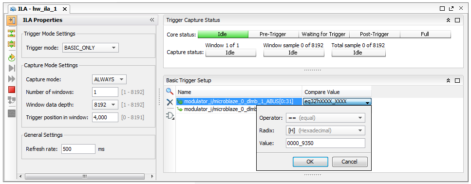
Illustration 4.30: Compare Value dialog box for the modulator_i/microblaze_0_dlmb_1_ABUS[3:31] ILA debug probe
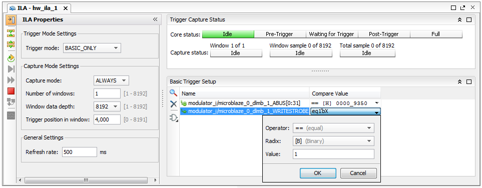
Illustration 4.31: Compare Value dialog box for the modulator_i/microblaze_0_dlmb_1_ WRITESTROBE ILA debug probe
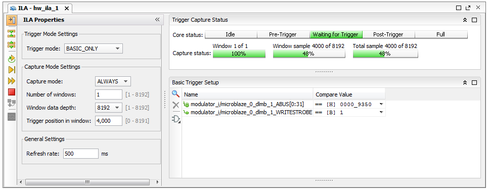
Illustration 4.32: ILA Properties window after arming trigger
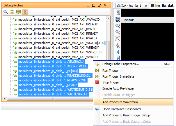
Illustration 4.33: Add Probes to Waveform option
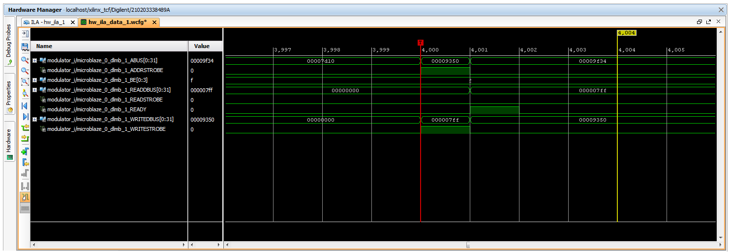
Illustration 4.34: Waveform Viewer
-
From the Illustration 4.34 we can see that in the moment when microblaze_0_dlmb_1_WRITESTROBE probe change its value from 0 to 1, data 000007ff (microblaze_0_dlmb_1_WRITEDBUS[0:31]) is being written into the memory location address 00009350 (microblaze_0_dlmb_1_ABUS[0:31]).
microblaze_0_dlmb_1_READY probe also changed its value from 0 to 1 which signalize that memory has finished one write transaction and it is ready for the next transaction.
If you want to check is correct data value (000007ff) written into the memory location address 0x9350, open the SDK tool and in the Memory tab you will find the correct data value, see Illustration 4.35.
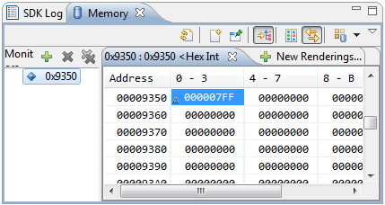
Illustration 4.35: Memory tab with data value on the memory address 0x9350
- To see the next data value that will be written in the next element of sine_ampl array, at memory location address 0x9354, arm the ILA core again and in the SDK tool press the Step Over command twice and check is the data value from the Memory tab equal to the data value shown in the Waveform Viewer.