1. INTRODUCTION
1.1 Motivation
Basic EDK Tutorial is a document made for beginners who are entering the embedded system design using FPGAs. This tutorial explains, step by step, the procedure of designing a simple digital system using C language and Xilinx Vivado Design Suite.
1.2 Purpose of this tutorial
This tutorial is made to introduce you how to create and test an project and run it on your development board.
After completing this tutorial, you will be able to:
- Launch and navigate the Vivado Integrated Design Environment (IDE)
- Create a MicroBlaze processor system project using Vivado IP Integrator tool
- Synthesize and implement the design in the Vivado IDE
- Export a hardware description XML file for later software development
- Create and debug your software application using SDK tool
- Generate the hardware implementation bitstream file and download it to the target Xilinx development board
-
Debug a design in hardware using Vivado Logic Analyzer
- Designing Surface: VIVADO 2014.2
- Programming Language: C
- Device: Xilinx Kintex-7 KC705 Evaluation Platform
1.3 Objectives of this tutorial
In this tutorial a PWM signal modulated using the sine wave with two different frequencies (1 Hz and 3.5 Hz) will be created. Frequency that will be chosen depends on the position of the two-state on-board switch (sw0).
PWM Signal
Pulse-width modulation (PWM) uses a rectangular pulse wave whose pulse width is modulated by some other signal (in our case we will use a sine wave) resulting in the variation of the average value of the waveform. Typically, PWM signals are used to either convey information over a communications channel or control the amount of power sent to a load. To learn more about PWM signals, please visit http://en.wikipedia.org/wiki/Pulse-width_modulation.
Illustration 1.1. illustrates the principle of pulse-width modulation. In this picture an arbitrary signal is used to modulate the PWM signal, but in our case sine wave signal will be used.
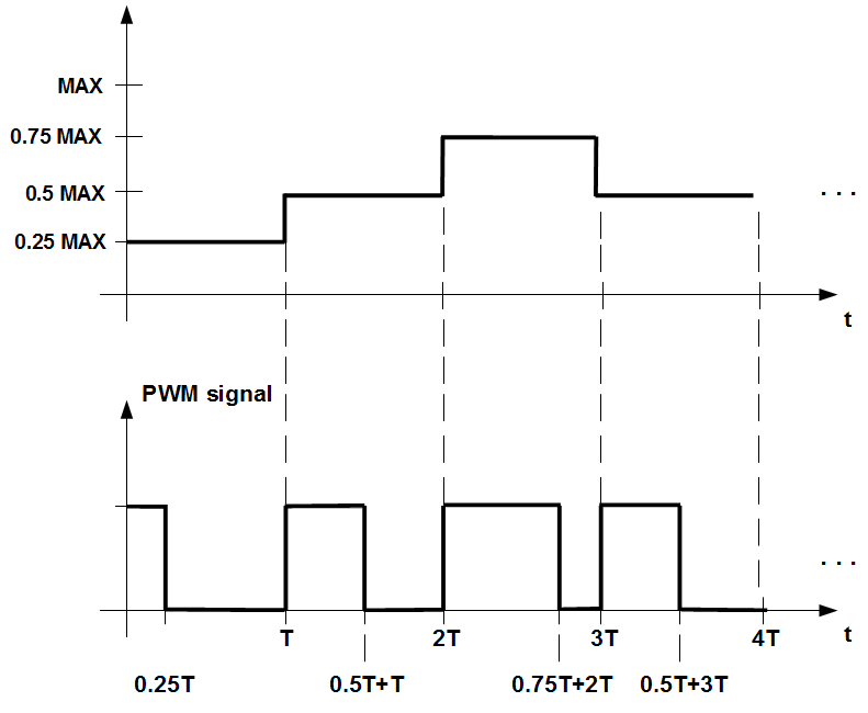
Illustration 1.1: Example of the PWM signal
1.4 One possible solution for the modulator design
Considering that we are working with digital systems and signals, our task will be to generate an digital representation of an analog (sine) signal with two frequencies: 1 Hz and 3.5 Hz.
Illustration 1.2 is showing the sine wave that will be used to modulate the PWM signal.

Illustration 1.2: Sine wave with 256 samples
One period of the sine wave is represented with 256 (28) samples, where each sample can take one of 4096 (212) possible values. Since the sine wave is a periodic signal, we only need to store samples of one period of the signal.
Note: Pay attention that all of sine signals with the same amplitude, regardless their frequency, look the same during the one period of a signal. The only thing that is different between these sine signals is duration of a signal period. This means that the sample rate of these signals is different.
Considering that the whole system will be clocked with the 100 MHz system clock, to get 1 Hz and 3.5 Hz frequencies (which is much smaller than 100 MHz) we should divide system clock frequency with integer value N.
In the Tables 1.1 and 1.2 are shown parameters that are necessary for generating sine signals with 1 Hz and 3.5 Hz frequencies.
Table 1.1: Sine signal with the frequency of 1 Hz
|
T=1 s |
T=1/1 Hz=1 s
|
T is the period of the signal |
|
f1=256 Hz |
f1=256*1 Hz=256 Hz (or read in time: 1 s/256)
|
f1 is the frequency of reading whole period (T) with 256 samples |
|
N1=390625 |
N1=100 MHz/256 Hz=390625
|
N1 is the number which divides frequency of the input clock signal (100 MHz) to the required frequency for the digital sine module |
|
N2=95 |
N2=390625/4096=95.3674 |
N2 is the number which divides frequency of the input clock signal (100 MHz) to the required frequency for the PWM's FSM module |
|
N1=389120 |
N1=95*4096=389120 |
This is new calculation, because N1 must be divisible with 4096 |
Table 1.2: Sine signal with the frequency of 3.5 Hz
|
T=0.286 s |
T=1/3.5 Hz=0.286 s
|
T is the period of the signal |
|
f2=896 Hz |
f2=256*3.5 Hz=896 Hz (or read in time: 0.286 s/256)
|
f2 is the frequency of reading whole period (T) |
|
N1=111607.1429 |
N1=100 MHz/896 Hz=111607.1428571
|
N1 is the number which divides frequency of the input clock signal (100 MHz) to the required frequency for the digital sine module |
|
N2=27 |
N2=111607.1428571/4096=27.2478 |
N2 is the number which divides frequency of the input clock signal (100 MHz) to the required frequency for the PWM's FSM module |
|
N1=110592 |
N1=27*4096=110592 |
This is new calculation, because N1 must be divisible with 4096 |
Now, it is obvious that the sine wave can be generated by reading sample values of one period, that are stored in one table, with appropriate speed. In our case the values will be generated using the sine function from the C numerics library (math.h) and will be stored in an array.
1.4.1 Block diagram
Block diagram on the Illustration 1.3 shows the structure of one possible system that can be used to generate required PWM signals.
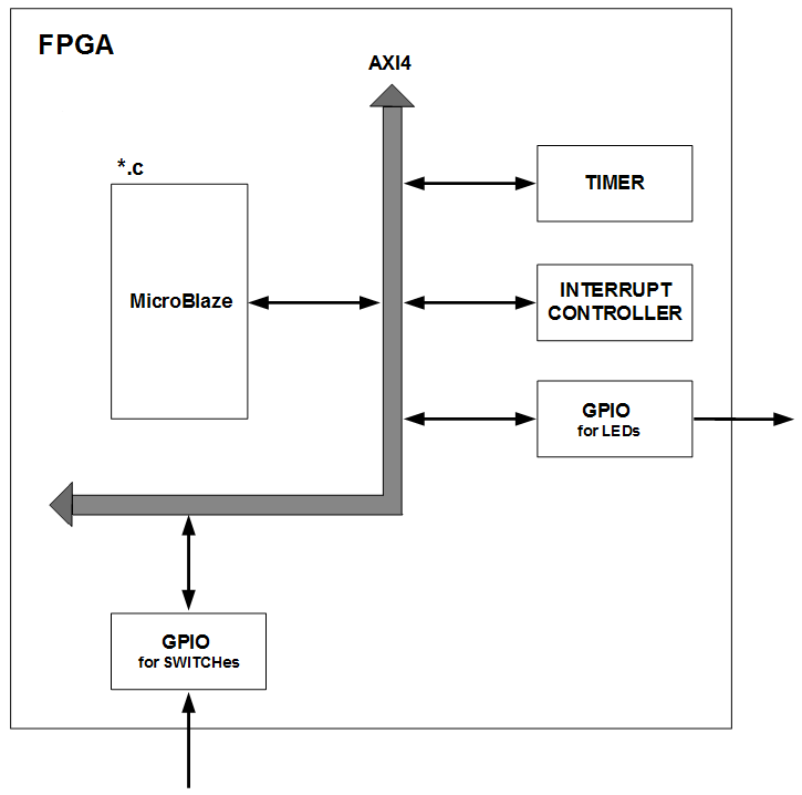
Illustration 1.3: Block diagram
The embedded system is composed of:
- MicroBlaze Processor core
- AXI Timer core
- AXI Interrupt Controller core
- AXI GPIO core to drive the LED
- AXI GPIO core to read the status of the SWITCH
Let us briefly explain each part of this system:
MicroBlaze Processor – is a 32-bit soft processor, which is included in the Vivado 2014.2 release. The MicroBlaze is highly configurable soft core processor, allowing you to select a specific set of features required by your design.
The fixed feature set of the processor includes:
- Thirty-two 32-bit general purpose registers
- 32-bit instruction word with three operands and two addressing modes
- 32-bit address bus
- Single issue pipeline
In addition to these fixed features, the MicroBlaze processor is parametrized to allow selective enabling of additional functionality:
- Hardware multiplier and divider
- Hardware debug logic
- Floating Point Unit (FPU)
- Memory Management Unit (MMU)
- OPB and LMB data and instruction side interface
- AXI4 data (M_AXI_DP) and instruction (M_AXI_IP) side interface
- AXI4 protocol for D-Cache (M_AXI_DC) and I-Cache (M_AXI_IC)
- AXI4 protocol for stream access
- etc...
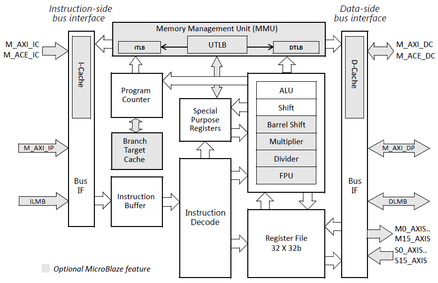
Illustration 1.4: MicroBlaze Core Block Diagram
The MicroBlaze core is organized as a Harvard architecture with separate bus interface units for data and instruction accesses. The following two memory interfaces are supported: Local Memory Bus (LMB) and the AMBA AXI4 interface (AXI4) and ACE interface (ACE). The LMB provides single-cycle access to on-chip dual-port block RAM. The AXI4 interfaces provide a connection to both on-chip and off-chip peripherals and memory. The ACE interfaces provide cache coherent connections to memory. MicroBlaze also supports up to 16 AXI4-Stream interface ports, each with one master and one slave interface.
MicroBlaze can be configured with the following bus interfaces:
- The AMBA AXI4 Interface for peripheral interfaces, and the AMBA AXI4 or AXI Coherency Extension (ACE) Interface for cache interfaces
- LMB provides simple synchronous protocol for efficient block RAM transfers
- AXI4-Stream provides a fast non-arbitrated streaming communication mechanism
- Debug interface for use with the Microprocessor Debug Module (MDM) core
- Trace interface for performance analysis
Note: If you want to read and learn more about the MicroBlaze Processor core, please refer to “MicroBlaze Processor reference Guide (v2014.1)”.
LogiCORE IP AXI Timer/Counter – The LogiCORE IP AXI Timer/Counter is a 32/64-bit timer module that interfaces to the AXI4-Lite interface. The AXI Timer is organized as two identical timer modules. Each timer module has an associated load register that is used to hold either the initial value for the counter for event generation or a capture value, depending on the mode of the timer.
The AXI Timer includes the following features:
- AXI interface based on the AXI4-Lite specification
- Two programmable interval timers with interrupt, event generation, and event capture capabilities
- Configurable counter width
- One Pulse Width Modulation (PWM) output
- Cascaded operation of timers in generate and capture modes
-
Freeze input for halting counters during software debug
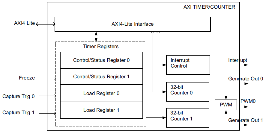
Illustration 1.5: AXI Timer Core Block Diagram
Note: If you want to read and learn more about the AXI Timer/Counter core, please refer to “LogiCORE IP AXI Timer v2.0 Product Guide”.
LogiCORE IP AXI Interrupt Controller (INTC) – The LogiCORE IP AXI Interrupt Controller (INTC) core receives multiple interrupt inputs from peripheral devices and merges them to a single interrupt output to the system processor. The registers used for storing interrupt vector addresses, checking, enabling and acknowledging interrupts are accessed through the AXI4-Lite interface.
The AXI Interrupt Controller includes the following features:
- Register access through the AXI4-Lite interface
- Fast Interrupt mode
- Supports up to 32 interrupts. Cascadable to provide additional interrupt inputs
- Single interrupt output
- Priority between interrupt requests is determined by vector position. The least significant bit (LSB, in the case bit 0) has the highest priority
- Interrupt Enable Register for selectively enabling individual interrupt inputs
- Master Enable Register for enabling interrupts request output
- Each input is configurable for edge or level sensitivity. Edge sensitivity can be configured for rising or falling. Level sensitivity can be active-high or active-low
- Output interrupt request pin is configurable for edge or level generation. Edge generation is configurable for rising or falling and level generation is configurable for active-high or active-low
- Configurable Software Interrupt capability
-
Support for nested interrupts
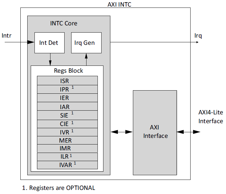
Illustration 1.6: AXI INTC Core Block Diagram
The LogiCORE IP INTC core concentrates multiple interrupt inputs from peripheral devices to a single interrupt output to the system processor. The registers used for checking, enabling, and acknowledging interrupts are accessed through the AXI4-Lite interface.
Note: If you want to read and learn more about the AXI Interrupt Controller core, please refer to “LogiCORE IP AXI Interrupt Controller (INTC) v4.1 Product Guide”.
LogiCORE IP AXI General Purpose Input/Output (GPIO) – The LogiCORE IP AXI General Purpose Input/Output (GPIO) core provides a general purpose input/output interface to the AXI interface. This 32-bit soft IP core is designed to interface with the AXI4-Lite interface.
The AXI GPIO includes the following features:
- Supports the AXI4-Lite interface specification
- Supports configurable single or dual GPIO channel(s)
- Supports configurable channel width for GPIO pins from 1 to 32 bits
- Supports dynamic programming of each GPIO bit as input or output
- Supports individual configuration of each channel
- Supports independent reset values for each bit of all registers
- Supports optional interrupt request generation
The AXI GPIO design provides a general purpose input/output interface to an AXI4-Lite interface. The AXI GPIO can be configured as either a single or a dual-channel device. The width of each channel is independently configurable.
The ports are configured dynamically for input or output by enabling or disabling the 3-state buffer. The channels can be configured to generate an interrupt when a transition on any of their inputs occurs.
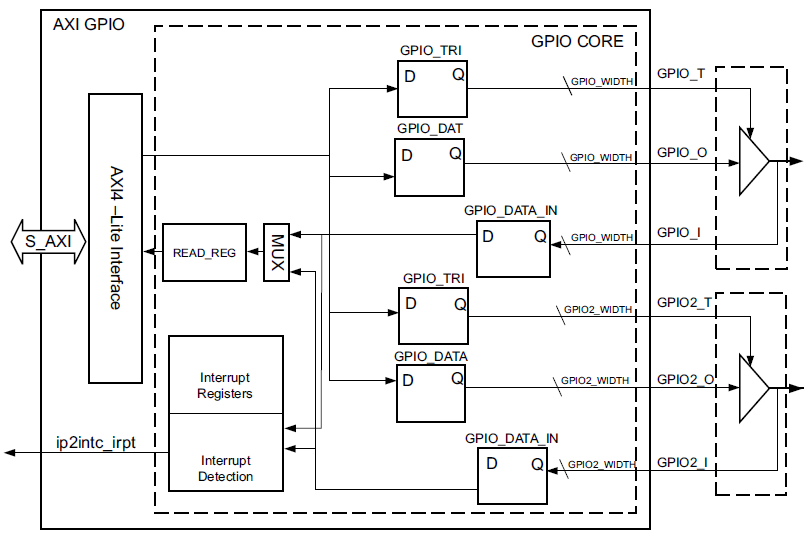
Illustration 1.7: AXI GPIO Block Diagram
Note: If you want to read and learn more about the AXI GPIO core, please refer to “LogiCORE IP AXI GPIO v2.0 Product Guide”.
1.4.2 Design Steps
This tutorial will be realized step by step with the idea to explain the whole procedure of designing an digital system, using Vivado tool.
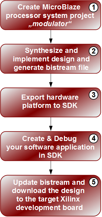
- - First, we will create a MicroBlaze processor system project (“modulator”) using Vivado IP Integrator tool. The block diagram of this system is shown on the Illustration 1.3. Here we will configure the selected microprocessor and peripherals, and specify the interconnections between these components.
- - After we create “modulator” project using Vivado IP Integrator tool, we will perform synthesis, implementation and bitstream file generation.
- - Then, we will export our hardware platform description to the Software Development Kit (SDK). The exported file has all the necessary information that SDK requires for software development and debug work on the hardware platform that we designed.
- - In the SDK, we will create and debug the software application for this project. There will be two different software applications, one without and one with the interrupt controller. Source codes for these two applications will be stored in modulator_no_intc.c and modulator_intc.c source file respectively.
- - Now, the design is ready to be implemented. The last step will be to initialize the bitstream with the appropriate ELF file and download it to the target Xilinx development board.
Illustration 1.8: Design steps
1.5 Embedded Design Process Flow
Vivado Design Suite is designed to help us in all phases of the embedded design process. On the Illustration 1.9 is shown the Vivado architecture structure of how the tools operate together to create an embedded system.
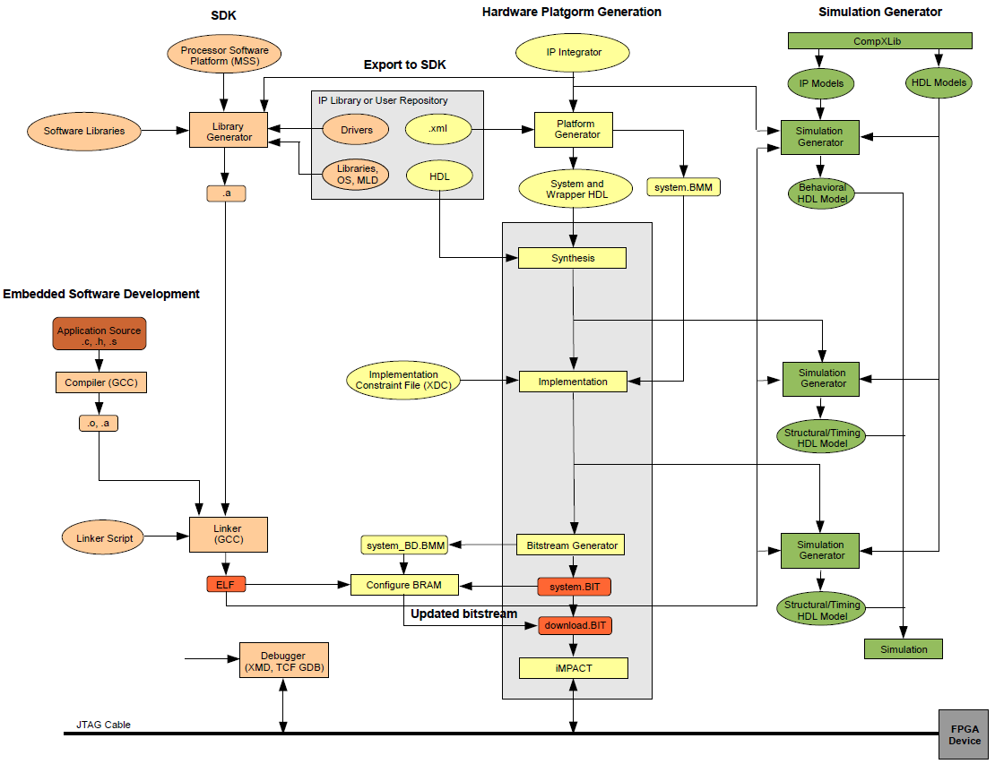
Illustration 1.9: Typical Embedded Design Process Flow